This web page belongs to a group of small projects that explore the features of the Smart Zynq board.
Introduction
There are several simple and low-cost DC servo motors on the market, for example SG90, MG90S, MG995 and MG996R. These motors are intended for hobby projects, in particular for building simple robots. Such motors are controlled by a single PWM signal.
Some motors rotate within a limited range of angles, typically 180 degrees. For such motors, the PWM signal controls the angular position of the motor. Other motors (often referred to as "360 degree motors") can rotate continuously. With such motors, the PWM signal controls the speed and direction of the rotation. Note that a motor model is often available in two variants: One variant with a limited angle, and a second variant that can rotate continuously. It's important to pay attention to this difference when purchasing a motor of this sort.
This tutorial shows how to connect up to eight servo motors to the Smart Zynq board and control these motors with the help of a simple Linux command. This tutorial also demonstrates how to use Xillybus' seekable streams for the purpose of implementing a register interface inside the FPGA.
The electrical wiring shown in this tutorial is suitable for only one motor, for the sake of keeping the descriptions and photos simple. Adding more motors is possible merely by adding wires to the same components as shown here.
The motor's electrical interface
The connection to servo motors of the relevant type consists of three wires:
- Brown wire, connected to ground.
- Red wire, connected to a +5V power supply.
- Orange wire, connected to the control signal (PWM).
The PWM signal needs to have a period time of 20ms (50 Hz). The duration at which the pulse is high controls the position or angular velocity of the motor.
According to most datasheets, the pulse's duration should be between 1ms and 2ms. This information is incorrect for some motors. For example, the correct range for Tower Pro's SG90 (having a 180 degree rotation limit) is between 500μs to 2450μs, approximately. This range corresponds to a 180 degree rotation. It's possible to rotate the motor slightly further with a pulse of up to 2560μs. This motor ignores a pulse longer than this.
So for the purpose of exploring the range of pulse durations that the motor responds to, it's better to experiment with the motor, rather than relying on the datasheet. As these motors are intended for hobby projects, their specification data may not be accurate.
Electrical connections
First of all, the servo motor needs a separate power supply in order to provide energy to the mechanical motor. The voltage for this power supply is +5V. It is not recommended to use the power supply that feeds the Smart Zynq board, because motors often cause sudden changes on the voltage level. The Smart Zynq board may behave unreliably if its power supply voltage is unstable.
The PWM signal on the orange wire should have approximately the same voltage as the power supply when this signal is high. In other words, the voltage between the orange wire and ground should be either 0 or approximately +5V.
The Smart Zynq board's output voltage is however only 3.3V when it's high. If such output is connected directly to the motor's orange wire, there is a good chance that the motor will respond correctly. The reason is that digital circuits that are based upon a 5V power supply usually consider any voltage above 2.5V as a logic '1'.
That said, it's uncertain if the motor will work reliably with a 3.3V voltage on the PWM signal. The recommended solution is to use a voltage level shifter that transforms the Smart Zynq board's into 0V or 5V. In this tutorial, a small board with the TXS0108E chip is used. This board merely exposes the chip's pins, so that ordinary wires can be connected to the chip.
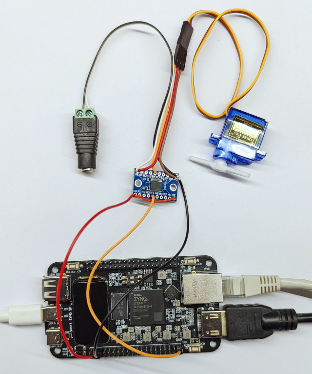
This picture shows how the electrical connections are arranged for controlling one servo motor: The Smart Zynq board at the bottom of the picture is connected to the TXS0108E Board with the help of Dupont wires. The other side of this board is connected to the servo motor's PWM input and as well as the separate power supply for the motors (through an adapter for a standard power supply plug). The motor's red and brown wires are also soldered to this board, in order to give the motor its power supply voltage.
This picture offers a closer look on the TXS0108E Board and its connections:
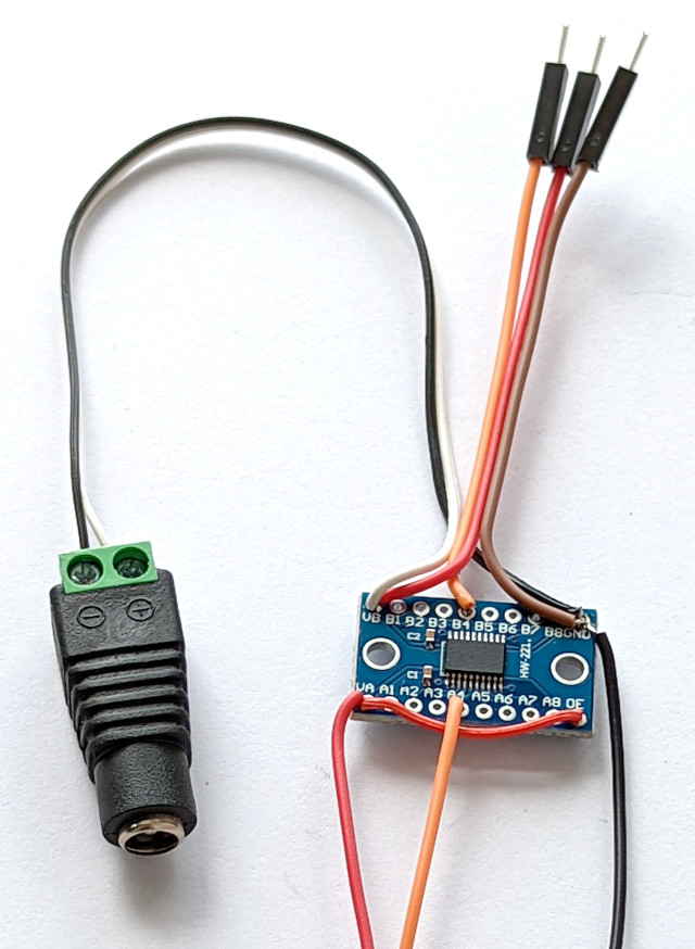
Pay attention to the red wire between OE and VA. This ensures that the chip's output enable is high.
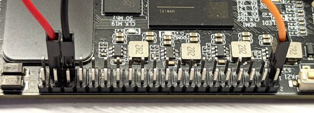
The connections to Smart Zynq's pin header are shown in the following picture. The motor is controlled by J6/1 as connected here.
This table summarizes the connections between the four parts involved:
| TXS0108E Board pin | Smart Zynq pin | Motor's wire | +5V power supply | Comment |
|---|---|---|---|---|
| VA | J6/37 (3.3V) | -- | -- | Also connected to OE |
| A4 | J6/1 | -- | -- | |
| OE | -- | -- | -- | Connected to VA |
| GND | J6/35 (GND) | Brown wire | GND | |
| VB | -- | Red wire | +5V | |
| B4 | -- | Orange wire | -- |
The TXS0108E chip performs a voltage level shift from its A4 input to its B4 output. There are seven additional pairs of pins on the chip. The A4/B4 pair was chosen arbitrarily for this tutorial. In order to control eight motors, all eight pin pairs of this chip can be used. This is not shown in here, because the amount of wires that is required for controlling eight motors would make the pictures difficult to understand.
In order to find the J6 pin header, look for where it's written "Bank 33 VCCIO Vadj" at the back side of the Smart Zynq board. The row of pins that is close to this marking is the pin header that is used in this tutorial. J6/1 is hence the pin that is closest to the HDMI connector.
Note that the Smart Zynq board is connected to a separate power supply through one of its USB ports. Also note that the J6 pin header's last pin is 5V, so don't connect a wire to this pin.
Preparing the Vivado project
Create a new Vivado project from the demo bundle's zip file (the boot partition kit). Open verilog/src/xillydemo.v in a text editor. Delete the part of the code that is labeled "PART 4". Instead of that part, insert this:
   assign  user_r_mem_8_empty = 0;
   assign  user_r_mem_8_eof = 0;
   assign  user_w_mem_8_full = 0;

   reg [7:0] reg0, reg1, reg2, reg3, reg4, reg5, reg6, reg7;

   always @(posedge bus_clk)
     if (user_w_mem_8_wren)
       case (user_mem_8_addr[2:0])
	 0: reg0 <= user_w_mem_8_data;
	 1: reg1 <= user_w_mem_8_data;
	 2: reg2 <= user_w_mem_8_data;
	 3: reg3 <= user_w_mem_8_data;
	 4: reg4 <= user_w_mem_8_data;
	 5: reg5 <= user_w_mem_8_data;
	 6: reg6 <= user_w_mem_8_data;
	 7: reg7 <= user_w_mem_8_data;
       endcase

   reg [7:0] mem_8_data_reg;
   assign user_r_mem_8_data = mem_8_data_reg;

   always @(posedge bus_clk)
     if (user_r_mem_8_rden)
       case (user_mem_8_addr[2:0])
	 0: mem_8_data_reg <= reg0;
	 1: mem_8_data_reg <= reg1;
	 2: mem_8_data_reg <= reg2;
	 3: mem_8_data_reg <= reg3;
	 4: mem_8_data_reg <= reg4;
	 5: mem_8_data_reg <= reg5;
	 6: mem_8_data_reg <= reg6;
	 7: mem_8_data_reg <= reg7;
       endcase

   servo_pwm servo_pwm_i [7:0]
     (
      .clk(bus_clk),
      .rst(quiesce),
      .pwm_signal(J6[7:0]),
      .pwm_width( { reg7, reg6, reg5, reg4, reg3, reg2, reg1, reg0 } )
      );
It's also possible to download the updated xillydemo.v from this link.
Create a new file, servo_pwm.v in the project's verilog/src/ directory, containing the following (use copy-paste or download from this link).
module servo_pwm
  (
   input clk,
   input rst,

   output reg pwm_signal,
   input [7:0] pwm_width
  );

   reg [9:0]  enable_count;
   reg 	      enable;

   reg [10:0] pwm_count;
   reg [8:0]  threshold;

   always @(posedge clk)
     begin
	if (enable_count == 999)
	  begin
	     enable_count <= 0;
	     enable <= 1;
	  end
	else
	  begin
	     enable_count <= enable_count + 1;
	     enable <= 0;
	  end

	threshold <= pwm_width + 50; // Add 0.5 ms to PWM width

	if (enable)
	  begin
	     if (pwm_count == 1999)
	       pwm_count <= 0;
	     else
	       pwm_count <= pwm_count + 1;

	     pwm_signal <= (pwm_count < threshold);
	  end

	if (rst)
	  begin
	     enable_count <= 0;
	     pwm_count <= 0;
	     pwm_signal <= 0;
	  end
     end
endmodule
Then add the file to the Vivado project: Click on File > Add Sources… and choose "Add or create design sources". Then click Next. Click on the "Add Files" button and choose the file named "servo_pwm.v" in the verilog/src/ directory. Then click the "Finish" button.
Create a bitstream file from the updated project in the same way that you created the bitstream file for the demo bundle. Also copy the bitstream file to the TF card in the same way (overwrite the old xillydemo.bit file with the file that was created with this project).
Controlling the servo motor
These steps shown in this section should be performed on a shell prompt on the Smart Zynq board.
First, change directory and perform a compilation of the demo applications for Xillybus:
# cd ~/xillybus/demoapps/
# make
gcc  -g -Wall -O3 memwrite.c -o memwrite
gcc  -g -Wall -O3 memread.c -o memread
gcc  -g -Wall -O3 streamread.c -o streamread
gcc  -g -Wall -O3 streamwrite.c -o streamwrite
gcc  -g -Wall -O3 -pthread fifo.c -o fifo
There are eight registers in the FPGA for the purpose of controlling the servo motor. Initially, their values are all zeros. This is how to print out these values in decimal format.
# hexdump -v -n 8 -e '8/1 "%u " "\n" ' /dev/xillybus_mem_8
0 0 0 0 0 0 0 0
A simpler hexdump command can be used to print out the same values in hexadecimal format:
# hexdump -v -n 8 -C /dev/xillybus_mem_8
00000000  00 00 00 00 00 00 00 00                           |........|
00000008
The memwrite program (inside the xillybus/demoapps/ directory) can be used to control the motor. For example, this command changes the value in register 0 to 120:
# ./memwrite /dev/xillybus_mem_8 0 120
This changes the rotation position or velocity of the motor that is connected to J6/1 (i.e. as shown in the photos above).
The width of the PWM pulse depends on value of this register according to this formula:
t = 500 + (x * 10)
In this formula, t is given in microseconds, and x is the value of the related register. The default width of the pulse is hence 500μs (i.e. for x=0). The command above changed the value of the register to 120. As a result, the pulse's width changed to 1700μs.
Each register consists of one byte, so its value ranges from 0 to 255. Accordingly, the pulse for each motor can be modified to have a width between 500μs and 3050μs. Note that part of this range of values is considered illegal by most motors. It's best to try different possibilities with each motor and see how it reacts.
In order to control a motor that is connected to another pin, write to a different register. For example, if the motor is connected to Smart Zynq's J6/4, this command can be used, for example:
# ./memwrite /dev/xillybus_mem_8 3 50
This command changes the width of the pulse to 1000μs (i.e. 1 ms).
After these two commands, the changes can be seen by reading back the values:
# hexdump -v -n 8 -e '8/1 "%u " "\n" ' /dev/xillybus_mem_8
120 0 0 50 0 0 0 0
This shows the values in decimal format. For hexadecimal format:
# hexdump -v -n 8 -C /dev/xillybus_mem_8
00000000  78 00 00 32 00 00 00 00                           |x..2....|
00000008
How memwrite works
The source code of memwrite is the file named memwrite.c in the ~/xillybus/demoapps/ directory. This program shows how to access registers with the help of Xillybus' seekable streams. If you want to understand how this program works, I suggest looking at the source code. I will only go through the two important parts below.
The program opens the file whose name is given in the first argument. The file descriptor for this file is stored in the variable @fd.
The program then performs a function call to lseek() as follows:
  if (lseek(fd, address, SEEK_SET) < 0) {
    perror("Failed to seek");
    exit(1);
  }
The variable @address contains the program's second argument. In the first example for using memwrite from above, this was 0. In the second example, it was 3. In general, lseek() is used to move to a specific position inside a file. In this case, the position in the file is the same as the number of the register that we want to access.
Next, the program makes a function call to allwrite():
allwrite(fd, &data, 1);
This writes one byte to the file. allwrite() is defined in memwrite.c, and is similar the well-known function write(). So instead of using allwrite(), this would be almost the same:
write(fd, &data, 1);
The difference is that write() doesn't ensure that the data is written. The function allwrite(), on the other hand, guarantees that the data is written to the file.
In this case, the function call to allwrite() writes that value of the program's third argument. In other words, this is the register's new value.
For more details about Xillybus' API for the host side, please refer to documentation on this subject, in particular section 6.1.
Explanation on the Verilog code
I shall first show how the Verilog code in xillydemo.v implements the registers inside the FPGA. This will be followed by the implementation of the PWM pulse.
Xillybus' API for implementing hardware registers is explained in detail in the Xillybus FPGA designer’s guide.
The wires related to the registers were already defined in the original xillydemo.v file:
  // Wires related to /dev/xillybus_mem_8
  wire  user_r_mem_8_rden;
  wire  user_r_mem_8_empty;
  wire [7:0] user_r_mem_8_data;
  wire  user_r_mem_8_eof;
  wire  user_r_mem_8_open;
  wire  user_w_mem_8_wren;
  wire  user_w_mem_8_full;
  wire [7:0] user_w_mem_8_data;
  wire  user_w_mem_8_open;
  wire [4:0] user_mem_8_addr;
  wire  user_mem_8_addr_update;
These wires are connected to the Xillybus IP core as part of its instantiation:
  xillybus xillybus_ins (

    // Ports related to /dev/xillybus_mem_8
    // FPGA to CPU signals:
    .user_r_mem_8_rden(user_r_mem_8_rden),
    .user_r_mem_8_empty(user_r_mem_8_empty),
    .user_r_mem_8_data(user_r_mem_8_data),
    .user_r_mem_8_eof(user_r_mem_8_eof),
    .user_r_mem_8_open(user_r_mem_8_open),

    // CPU to FPGA signals:
    .user_w_mem_8_wren(user_w_mem_8_wren),
    .user_w_mem_8_full(user_w_mem_8_full),
    .user_w_mem_8_data(user_w_mem_8_data),
    .user_w_mem_8_open(user_w_mem_8_open),

    // Address signals:
    .user_mem_8_addr(user_mem_8_addr),
    .user_mem_8_addr_update(user_mem_8_addr_update),

[ ... ]

    .quiesce(quiesce)
  );
Next, we look at the Verilog code that was added specifically for this project. It starts with this part, which makes sure that no flow control is applied on the exchange of data with the host:
   assign  user_r_mem_8_empty = 0;
   assign  user_r_mem_8_eof = 0;
   assign  user_w_mem_8_full = 0;
The eight registers are declared next:
reg [7:0] reg0, reg1, reg2, reg3, reg4, reg5, reg6, reg7;
The next part implements write operations to the registers: When @user_w_mem_8_wren is high, a new value is written to one of the registers. @user_mem_8_addr selects which register is affected. Both @user_w_mem_8_wren and @user_mem_8_addr are outputs of the Xillybus IP core.
   always @(posedge bus_clk)
     if (user_w_mem_8_wren)
       case (user_mem_8_addr[2:0])
	 0: reg0 <= user_w_mem_8_data;
	 1: reg1 <= user_w_mem_8_data;
	 2: reg2 <= user_w_mem_8_data;
	 3: reg3 <= user_w_mem_8_data;
	 4: reg4 <= user_w_mem_8_data;
	 5: reg5 <= user_w_mem_8_data;
	 6: reg6 <= user_w_mem_8_data;
	 7: reg7 <= user_w_mem_8_data;
       endcase
After this, the possibility to read values from these registers is implemented: When @user_r_mem_8_rden is high, @user_r_mem_8_data is updated so it contains the value of one of the registers. @user_mem_8_addr selects which register's value is read.
   reg [7:0] mem_8_data_reg;
   assign user_r_mem_8_data = mem_8_data_reg;

   always @(posedge bus_clk)
     if (user_r_mem_8_rden)
       case (user_mem_8_addr[2:0])
	 0: mem_8_data_reg <= reg0;
	 1: mem_8_data_reg <= reg1;
	 2: mem_8_data_reg <= reg2;
	 3: mem_8_data_reg <= reg3;
	 4: mem_8_data_reg <= reg4;
	 5: mem_8_data_reg <= reg5;
	 6: mem_8_data_reg <= reg6;
	 7: mem_8_data_reg <= reg7;
       endcase
Finally, the instantiation of the servo_pwm module takes place.
   servo_pwm servo_pwm_i [7:0]
     (
      .clk(bus_clk),
      .rst(quiesce),
      .pwm_signal(J6[7:0]),
      .pwm_width( { reg7, reg6, reg5, reg4, reg3, reg2, reg1, reg0 } )
      );
Note that this instantiation creates eight identical copies of servo_pwm: The first copy is connected to reg0 and J6[0], the second copy is connected to reg1 and J6[1] etc.
We shall now look at the servo_pwm module. It starts with declaring the module's ports and registers:
module servo_pwm
  (
   input clk,
   input rst,

   output reg pwm_signal,
   input [7:0] pwm_width
  );

   reg [9:0]  enable_count;
   reg 	      enable;

   reg [10:0] pwm_count;
   reg [8:0]  threshold;
Recall from before that @pwm_signal receives the value of the register, which is updated with the help of the memwrite command on the host. @pwm_signal is connected to the Smart Zynq board's pin, so this is the signal that arrives to the motor on the orange wire.
The next part of this module implements a strobe signal: @enable is high once in every 1000 clock cycles. @clk's frequency is 100 MHz. Hence @enable is high once in every time period of 10μs.
   always @(posedge clk)
     begin
	if (enable_count == 999)
	  begin
	     enable_count <= 0;
	     enable <= 1;
	  end
	else
	  begin
	     enable_count <= enable_count + 1;
	     enable <= 0;
	  end
As mentioned earlier, the register's value range from 0 to 255 corresponds to a PWM pulse width between 500μs and 3050μs (the expression for the pulse's width in microseconds was 500 + x * 10).
Hence this is the expression for @threshold.
threshold <= pwm_width + 50; // Add 0.5 ms to PWM width
This register contains the number of times @enable is high during the PWM pulse (i.e. when the PWM signal is high). This expression reflects the fact that the value of the register is the length of the PWM pulse in units of 10μs. Adding 50 to the register's value corresponds to the minimal pulse width of 500μs.
@enable is now used as a clock enable for this part:
	if (enable)
	  begin
	     if (pwm_count == 1999)
	       pwm_count <= 0;
	     else
	       pwm_count <= pwm_count + 1;

	     pwm_signal <= (pwm_count < threshold);
	  end
@pwm_count counts from 0 to 1999 and starts over again. This counter changes only once in every 10μs, so it completes a full round every 20000μs = 20 ms. In other words, the PWM pulse's repeat cycle is 20ms, as required.
@pwm_signal is high as long as @pwm_count is smaller than @threshold. This is how the pulse's width is controlled by the register.
The final part in this module consists of resetting some registers:
	if (rst)
	  begin
	     enable_count <= 0;
	     pwm_count <= 0;
	     pwm_signal <= 0;
	  end
     end
endmodule
When @rst if high, this part overrules anything written above. Hence @rst has the function of a reset signal.
The relation between Verilog code and real pins
The Verilog code above uses the inout port named J6, but how do the connections with this port reach the pin header? The answer can be found in xillydemo.xdc. This file is part of the Vivado project that creates the bitstream (in the "vivado-essentials" directory).
xillydemo.xdc contains various information that is necessary for the FPGA to work properly as an electronic component. Among others, this file contains these rows:
[ ... ]

## J6 on board (BANK33 VADJ)
set_property PACKAGE_PIN U22  [get_ports {J6[0]}];   #J6/1  = IO_B33_LN2
set_property PACKAGE_PIN T22  [get_ports {J6[1]}];   #J6/2  = IO_B33_LP2
set_property PACKAGE_PIN W22  [get_ports {J6[2]}];   #J6/3  = IO_B33_LN3
set_property PACKAGE_PIN V22  [get_ports {J6[3]}];   #J6/4  = IO_B33_LP3
set_property PACKAGE_PIN Y21  [get_ports {J6[4]}];   #J6/5  = IO_B33_LN9
set_property PACKAGE_PIN Y20  [get_ports {J6[5]}];   #J6/6  = IO_B33_LP9
set_property PACKAGE_PIN AB22 [get_ports {J6[6]}];   #J6/7  = IO_B33_LN7
set_property PACKAGE_PIN AA22 [get_ports {J6[7]}];   #J6/8  = IO_B33_LP7

[ ... ]
The first row says that the port J6[0] should be connected to U22. This is a position on the FPGA's physical package. According to Smart Zynq's schematics, this FPGA pin is connected to the first pin of the pin header. The positions of the other ports are defined in the same manner.
Summary
This tutorial showed how to control servo motors with the help of the Smart Zynq board and Xillybus' register API. The host application as well as the Verilog code for this application were presented.
This tutorial can also serve as a basis for other applications requiring the control of hardware with the help of registers.