This page is the fifth in a series of pages introducing the Multi-Gigabit Transceiver (MGT). After going through a lot of topics (and listing some protocols for FPGAs), it's time to look at how the PMA turns the data into an electrical signal and vice versa.
Introduction
The PMA consists of the parts in the MGT that are related to the physical channel. Most notable, the serializer and deserializer are part of the PMA. In other words, the conversion of the physical channel's bits from and to a parallel word occurs inside the PMA.
The PMA is also the part that converts the bits into electrical voltages. Likewise, this is the part that receives the electrical voltages from the MGT on the other side and converts this into bits.
Another important role of the PMA is to compensate for the distortion of the voltage signal that occurs as this signal travels between the two MGTs:
- The transmitter may intentionally distort the analog signal that it creates for transmission. The transmitter's distortion is an attempt to do the opposite to what the physical channel does to the signal. This is often referred to as pre-emphasis.
- The receiver's equalizer may manipulate the arriving analog signal in order to mitigate the distortion causes by the physical channel.
This page introduces these functionalities. The PMA is also responsible for other tasks that are relevant only when the data stream is turned off. These topics are discussed on the next page.
This is the block diagram of a typical MGT, shown here again to display the PMA's position in the larger context (this diagram is the same as on the previous page).
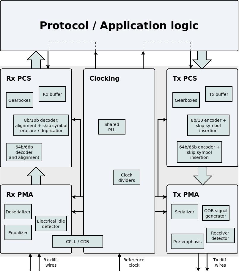
Also similar to the previous page, I shall use the expressions Tx PMA and Tx PCS in relation to the parts in the MGT that are used for transmitting data. Likewise with Rx PMA and Rx PCS for receiving data.
It's important to note that in the vast majority of usage scenarios, there is no need to understand anything about the physical channel, how it distorts the signal and how this distortion is corrected. Usually, all that you need to know is that using the equalizer is a good idea.
That said, it's important to be aware that the PMA is an analog component to a large extent. The MGT usually has separate power supply pins on the FPGA chip. Some of these pins feed the PMA with power. The voltage on these pins is often required to be cleaner than usual. Failing to meet these requirements may degrade the MGT's performance significantly.
For the sake of the explanations below, we shall look at a 5 Gb/s communication link. This is the data rate used by protocols like SuperSpeed USB Gen 1 and PCIe 2.0. We shall also assume that the parallel word that is used between the PMA and the PCS is 32 bits wide. I'll start with a simplified description of the physical channel, omitting some details that are discussed further down this page.
Transmitting data
The Tx PMA converts the parallel word into an electrical signal by transmitting the parallel word starting from the LSB. Accordingly, if bit 0 is a '1', the Tx PMA adjusts its output pins so that the voltage between D+ and D- is 500 mV (for example). If this bit is a '0', this voltage is -500 mV (negative).
The Tx PMA waits for 0.2 ns, and then does the same with bit 1 of the parallel word. In other words, the voltage between D+ and D- will be either 500 mV or -500 mV, depending on bit 1. This way, each of the bits of the parallel word is represented at the output pins for a time period of 0.2 ns. After 6.4 ns, the entire parallel word has been transmitted on the wires. The Tx PMA receives a new parallel word from the Tx PCS, and starts transmitting its value in the same way.
The transfer of the parallel word from the Tx PCS to the Tx PMA is synchronized with a clock (often named XCLK). In this example, the clock cycle of this clock is 6.4 ns, so its frequency is 156.25 MHz. Not surprisingly, 156.25 × 32 = 5000.
What I've described here is the transmitter side of a SERDES. The time allocated for each bit of this SERDES' output is 0.2 ns, which results in a data rate of 5 Gb/s.
In this example, the voltage between the two differential output pins was 500 mV. This is within the allowed range for PCIe and SuperSpeed USB. Note that protocol specifications as well as MGT's datasheets usually specify this voltage in terms of differential peak-to-peak voltage. This is the difference between the lowest and highest differential voltage, i.e the difference between -500 mV and 500 mV in this example. So for this example, the differential peak-to-peak voltage is 1000 mV. This is the number that will usually appear in the specifications and datasheets.
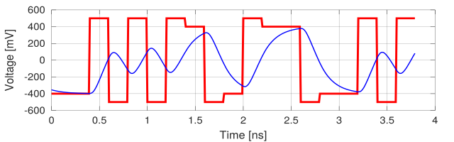
But the signal has changed by the time it arrives the receiver. The image below shows an example of the analog signal's waveform:
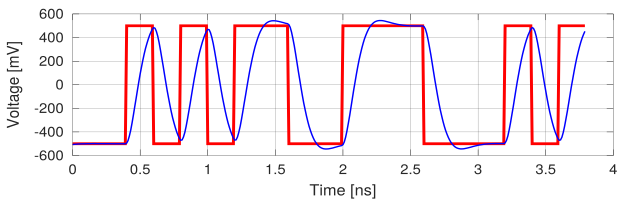
The transmitter's output (the voltage between D+ and D-) is shown in red. The blue waveform is an example of how this signal can arrive to the receiver. This example shows a simulation of a simple low-pass filter with a bandwidth of 2.5 GHz.
Throughout this page, I shall rely on this example with a data rate of 5 Gb/s and a differential voltage of 500 mV. Other numbers are of course possible: An FPGA MGT allows controlling the data transmission rates and the output voltages.
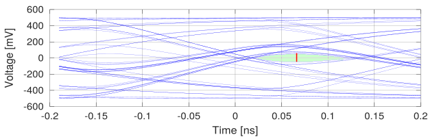
The eye diagram
The waveforms in the image above demonstrate that the signal that arrives to the receiver is different from the signal generated by the transmitter. The eye diagram is a graphical representation of the signal that arrives to the receiver. This graph is created by drawing several waveforms on the same axes. Each such waveform is the result of a random combination of transmitted bits. Hence the overlapping waveforms on the graph represent all possible shapes of the arriving signal.
This is the eye diagram for the same scenario as the image above:
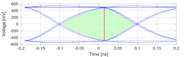
This image explains why this is called an "eye diagram". The green area in the middle has the shape of an eye.
The red line shows the optimal timing for measuring the voltage for the purpose of deciding whether the transmitted bit is a '0' or a '1'. The voltage difference is largest at this time, so this is where the immunity to noise is best. Note that the chosen moment is slightly after zero. Compare this with the previous image: The bit that is detected at this moment in time has already been transmitted during 0.2 ns, and the detection occurs even slightly later.
The eye diagram is commonly used in order to assess the quality of the signal arriving to the receiver. This graph is often created in simulations of the physical media that transports the signal. It's also possible to obtain an eye diagram from measurements of a real signal with the help of an oscilloscope or more specialized measurement equipment.
Receiving data
The Rx PMA converts an electrical signal into a parallel word: The Rx PMA measures the voltage between its two input pins (D+ and D-) once every time period of 0.2 ns. If this voltage is positive, bit 0 of the parallel word is assigned a '1'. Otherwise, this bit is '0'. The Rx PMA continues to assign values to the other bits of the parallel word, from bit 1 until bit 31. When the parallel word is completed, the Rx PMA hands it over to the Rx PCS. So the Rx PMA is a mirror image of the Tx PMA.
But how does the Rx PMA know exactly when to measure the voltage of its input pins? This should happen once in every time period of 0.2 ns, but when exactly inside this time period? How does the Rx PMA know the optimal timing that was shown as the red line in the eye diagram above?
To make things even more complicated, the Rx PMA often doesn't have access to the reference clock that the Tx PMA relies upon. The receiver's perception of how long time 0.2 ns lasts is therefore not exactly the same as the transmitter's view on the same question. Also, this reference clock's frequency changes randomly all the time due to jitter. And for protocols that require SSC (Spread Spectrum Clock), this clock's frequency deliberately varies continuously according to a predefined pattern.
The solution to this problem is Clock Data Recovery (CDR). This is a mechanism inside the Rx PMA that finds the optimal timing for sampling the voltage at the input pins. The CDR generates a sampling clock that adapts itself to the arriving data stream. This clock is divided by 32 (in this example) for the purpose of generating the clock used to interface with the Tx PCS.
The CDR is sensitive to transitions between '0' and '1' in the arriving analog signal. More precisely, the CDR detects when the voltage between the two differential pins changes between positive and negative. This allows the CDR to adapt the frequency of the sampling clock that it generates to the clock that is used by the transmitter.
In order to operate properly, the CDR needs a reference clock of its own. This reference clock's a frequency must be approximately the same as the transmitter's clock frequency. However, this reference clock is only used for the initial synchronization with the data stream. After this initial synchronization, the CDR follows the transmitter's frequency with the help of a PLL. This adaptive mechanism continuously changes the sampling clock's frequency slightly in order to create a replica of the transmitter's clock. In addition to that, the CDR also strives to move sampling moment to the optimal point, within each period of 0.2 ns. In other words, the CDR attempts to ensure that the sampling of the signal occurs at the red line in the eye diagram shown above.
The CDR plays a crucial role in obtaining a reliable communication link. For example, if the transmitter uses a low-quality reference clock that has a high level of jitter, this will add randomness to the length of each bit's time period. If the receiver's CDR is unable to adapt to this randomness quickly enough, sampling will occur at non-optimal positions. As a result, the probability for errors increases. It's also possible that the CDR loses synchronization completely, causing a temporary loss of the communication link. Situations of this sort are often mistaken for problems with the signal integrity of the data wires rather than a low-quality clock.
In an FPGA MGT, the CDR's behavior depends on several parameters that can be configured. Unfortunately, the meaning of these parameters is usually complicated and undocumented. The FPGA tools choose the values for these parameters automatically based upon the MGT's settings. This relies in particular on the data rate. If a specific well-known protocol is selected, the CDR's parameters are chosen accordingly. It sometimes pays off to test different settings in order to obtain a more stable link, in particular if there are low-quality cables and connectors along the connection between the two MGTs.
Reversal of polarity
Both the Rx PMA and Tx PMA support the possibility to reverse the polarity of the physical channel. This means transmitting a '0' instead of a '1' and vice versa. Or receiving a '1' when a '0' would normally be received, and vice versa.
In other words, if the D+ and D- wires are swapped, the MGT can compensate for this. This is a trivial but yet very important features that often simplifies the PCB design.
Signal distortion
In a perfect world, the voltage signal from the transmitting MGT would arrive to the receiving MGT without any change. In reality, there signal undergoes several changes until it arrives to its destination. The most notable problem is the filtering property of the signal path: Every time the Tx PMA transmits an '0' after a '1', there is a sharp transition from positive voltage to negative voltage. The opposite happens, of course, in a transition from '0' to '1'. This sharp voltage change is distorted by the physical medium that carries the signal. Cables and PCB traces behave like a low-pass filter.
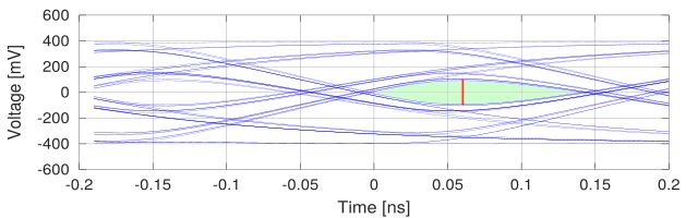
This image shows the same as example of waveforms from above, but with a simulation of a more difficult physical channel:
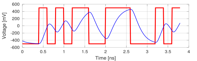
The blue waveform shows how the voltage that arrives to the receiver "remembers" the values of a few bits that were transmitted earlier. Recall from before that the receiver needs to decide on a '0' or '1' depending on whether the voltage is negative or positive. Hence the values from previous bits interfere with the receiver's decision. The fact that one bit's value interferes with the receiver's decision on another bit is called Inter-Symbol Interference (ISI).
The eye diagram for the same simulation of the physical channel:
This eye diagram shows that it is still possible to tell the difference between a '0' and a '1', but the margin is much smaller. In other words, much less noise is required to cause an error.
Aside from the effect that is simulated in the eye diagram above, the signal is distorted in other ways as well:
- The signal loses energy as it travels to the receiver, so the voltage between the differential wires becomes lower than transmitted.
- Reflections are added to the signal as it travels from the transmitter to the receiver. This effect is similar to an acoustic echo, and it occurs in particular when the signal passes through a connector or another kind of abrupt discontinuity of the conducting medium.
- Noise is added to the signal from various external sources. This is usually not a dominant factor in communication between MGTs, as the effects from distortions are usually more significant. But noise this can be significant with a long a poorly isolated cable.
We shall now look at two mechanisms for mitigating the physical channel's signal distortion: The equalizer, which is part of the receiver, and pre-emphasis, which is part of the transmitter.
Equalizer
The equalizer manipulates the analog signal that arrives to the MGT. The purpose of this unit is to mitigate the effects of the physical channel's signal distortion. By doing so, the equalizer reduces the channel's bit error probability and allows for a higher data rate. The equalizer is always the first step of the Rx PMA's processing chain.
There are mainly two kinds of equalizers in use. An MGT may support both:
- LPM (Low Power Mode). This equalizer usually consists of a high-pass filter that compensates for the physical channel's tendency to attenuate the higher part of the analog signal's spectrum. Some MGTs adapt this filter automatically to the received signal. With less advanced MGTs, the application logic is required to select one filter out of several possibilities.
- DFE (Decision Feedback Equalizer), explained in more detail below.
Recall from the example above that the Rx PMA measures the voltage between its two input pins (D+ and D-) once every time period of 0.2 ns. Based upon whether this voltage is negative or positive, the Rx PMA detects a '0' or a '1'. When an equalizer is used, the Rx PMA relies on the output of the equalizer instead.
If the DFE is used, it's assumed that the transmitter ensures that the transmitted bits are statistically independent of each other. What if the physical channel doesn't distort the signal? In this case, the voltages that the Rx PMA uses to decide on a '0' or a '1' are also mutually statistically independent. In other words, each time the Rx PMA examines its analog input signal, there should be no statistical relation to neither the previous signals nor the future signals.
But in reality, the physical channel distorts the signal carrying the data stream. Therefore, there is a statistical relation between the voltages that represent a '0' or a '1': The low-pass filter effect smears the voltage signal, and reflections ("echoes") also reduce the signal's quality. Each bit's voltage level spills over to the neighboring bits. As mentioned above, this effect is called Inter-Symbol Interference (ISI). If the receiver does nothing to mitigate the ISI's effect, this mutual interference between bits is equivalent to adding noise to the channel.
The DFE works similar to an echo canceler: It consists of a filter that adjusts itself in order to remove any correlation between the samples that represent '0' or '1'. More precisely, it removes the correlation between the detected bits ('0' or '1') and the analog signals that belong to the neighboring bits. In other words, if the DFE has achieved its goal, there is no statistical correlation between the analog signal that is used to decide on a bit's value and other bit's values. In this case, the ISI is reduced to zero, which means that the channel's smearing effect and reflections have no impact on the quality of transmission.
Note that if there is a statistical correlation between the bits that are transmitted on the channel, the DFE will attempt to eliminate this correlation. As a result, the DFE will adjust the analog filter in a way that doesn't correspond to the physical channel's distortion of the analog signal. Hence the DFE will distort the signal rather than repairing it. This is the reason why a scrambler is always required when DFE is activated.
If there is no way to ensure that the transmitted bits are mutually uncorrelated, the LPM equalizer may be suitable. The MGT's datasheet usually states if the LPM equalizer can be used without a scrambler.
Not all MGTs have an DFE, but almost all MGTs have an LPM equalizer of some sort. The information in datasheets is often incomplete regarding what kind of equalizers the MGT supports, and how these equalizers work. If the datasheet says nothing about the type of the equalizer, it's most likely an LPM.
Even though DFE is a more sophisticated type of equalizer, it doesn't always perform better than LPM, even if the bits are mutually uncorrelated. In particular, when the quality of the physical channel is relatively high, LPM may perform better than DFE.
Pre-emphasis
It can be helpful to manipulate the transmitter's output signal in a way that improves the signal that arrives to the receiver. This method is called pre-emphasis, and is in particular useful if the signal's distortion is so severe that the receiver can't synchronize on the data stream at all. There are several variants for this method, and each MGT has its own set of features.
In most situations, the physical channel has the effect of a low-pass filter. The transmitter can proactively compensate for some of the channel's distortion by shaping the transmitter's output signal. The simplest mechanism is post-cursor emphasis: Since the physical channel reacts slowly to changes in the transmitter's output, the transmitter compensates for this by applying a higher voltage when the bit changes. Or more precisely, the transmitter reduces the voltage when the bit doesn't change.
To demonstrate this mechanism, recall that in the example from above, the transmitter's output was either -500 mV or 500 mV (for a '0' or '1').
With post-cursor emphasis, if the output changes from '0' to '1' the transmitter's output will be 500 mV just like before. But if the next bit is '1' again, the output voltage is lower, for example 400 mV. The same thing happens for transitions from '1' to '0'. In this case, the output voltage will be -500 mV. But if the next bit is '0' again, the voltage will be -400 mV.
This image shows the same simulation as the last image with waveforms, but with post-cursor emphasis applied:
The red waveform shows how post-cursor emphasis works: The output voltage gets a small boost every time the bit changes, and resumes to a lower voltage otherwise. This method is often called de-emphasis, because the transmitter reduces the voltage of repeated bits, so these bits are "less emphasized".
Comparing the blue waveform with the the image above, it's evident that this voltage's swing is smaller. This may not seem like a big deal, but the difference is more evident on the eye diagram:
This is clearly better, but not good enough: An equalizer is still needed in a scenario like this.
Note that post-cursor emphasis can be described as a simple FIR filter. Denote the voltages of the transmitter without emphasis as x(n) (n is the number of the bit that is transmitted). Each x(n) can have the value -500 mV or 500 mV. The output of the transmitter with post-cursor emphasis can hence be written as follows:
y(n) = 0.9 x(n) - 0.1 x(n-1)
This is a simple expression for an FIR filter, which favors high-frequency signals. This can be seen as a compensation for the physical channel's behavior as a low-pass filter.
The "post-cursor" part in the expression "post-cursor emphasis" relates to the fact that the corresponding FIR filter can be written as:
y(n) = (1-a) x(n) - a x(n-1)
In this expression, a is usually chosen as a positive number.
This FIR filter basically says: The value of y(n) mostly depends on x(n), but if x(n-1) had the same value, y(n) is a little closer to zero. y(n)'s manipulation depends on the previous bit.
Hence the word "cursor" relates to the currently transmitted bit. The word "post" refers to the fact that this filter depends on on the previously transmitted bit, i.e. the bit after the "cursor".
It's possible to generalize the idea of a FIR filter that is more favorable to high-frequency signals. In particular, this FIR is often implemented in MGTs:
y(n) = apre x(n+1) + a0 x(n) - apost x(n-1)
In this expression, apost relates to the post-cursor emphasis that has already been presented. apre represents the dependency on the bit before the "cursor", i.e. pre-cursor emphasis, sometimes also called preshoot. This should not be confused with the term pre-emphasis, which covers the whole range of manipulations of the transmitter's output signal that can be represented with a FIR filter.
Each MGT offers different possibilities to shape the transmitted signal. post-cursor emphasis is usually available because several protocols require it. As for other variations, it depends on the MGT.
The obvious drawback with pre-emphasis is that the results of the transmitter's adjustments are visible only to the receiver. Recall that the equalizer can adjust itself continuously to attain optimal reception. But in general, the pre-emphasis mechanism doesn't know how well the signal is received on the other side. The can be solved by the protocol. For example, the Displayport protocol specifies a mechanism that allows the receiving side to send requests to the transmitter. This way, the receiver controls the transmitter's voltage level and the level of post-cursor emphasis.
Pre-emphasis is also useful when the physical channel is known in advance, for example when two FPGAs are connected to each other on a PCB. It can nevertheless be a good idea to use pre-emphasis even when the channel's parameters are unknown, in particular with high data rates (8 Gb/s and above).
Note that the pre-emphasis mechanism and the equalizer are not substitutes for each other, even though both are filters that improve the signal quality and reduce errors. The equalizer is usually the stronger tool between these two. The pre-emphasis' role should be to help the equalizer or to ensure that the signal quality is good enough to allow the receiver to synchronize with the transmitter.
Pre-emphasis is not used at all in many applications. This tool is useful in particular when the distance between the two MGTs is long, and in particular when the signal travels on a PCB. When the distance is reasonably short and the receiver is equipped with a good equalizer, there is usually no reason to manipulate the transmitter's output signal.
Statistical eye scan
It is often desired to evaluate the channel's quality, even when all data arrives without errors. In particular, it's interesting to know how far away the channel is from starting to produce errors. Is the channel robust, or will errors begin if the smallest change occurs with the physical media?
Also, recall from the previous page that when the channel is used for transmitting useful data, a BER test is not possible at the same time. It is therefore difficult to assess the channel's quality while it is used (except for some protocols that report all errors, e.g. xillyp2p).
The common way to assess a link's quality is to measure the eye diagram at the receiver. This can be done when the signal arrives with a cable and a connector: There is measurement equipment for this purpose (which is quite expensive). However when the signal travels on a PCB and arrives to a chip (an FPGA in particular) there is usually no place to pick up the signal from. Using a probe to touch a wire on the PCB will result in a dramatic change in the signal's shape, so the measurement will be worthless.
The elegant solution to this problem is a statistical eye scan. This means that the Rx PMA itself measures the signal's eye diagram. This method has several advantages:
- The signal is measured exactly at the point where the Rx PMA decides on a '0' or a '1'.
- The measurement doesn't alter the signal.
- The measurement includes the equalizer's correction. It hence helps choosing which equalizer to use, and to fine-tune its parameters.
- If the CDR isn't able to cope with the jitter of the transmitter's clock, this is visible in this measurement.
- The measurement doesn't interfere with the Rx PMA's normal operation. It's therefore possible to test the channel while it is used to transport real data.
There is only one disadvantage with this method: Its result isn't really an eye diagram. But the result is almost equally as useful.
Recall from above that the Rx PMA decides if the received signal is a '0' or a '1' based upon if the differential voltage of the arriving signal is negative or positive. The CDR is responsible for making this decision with the optimal timing.
For the purpose of statistical eye scan, there an additional unit that makes the decision on '0' or '1'. However this second unit makes its decision slightly earlier or slightly later than the first unit. This time offset is controlled by setting the MGT's registers (this can be done while the MGT is working).
Another difference between the two units is how they decide if the signal is a '0' or a '1': As already mentioned, the first unit compares the signal's voltage with zero. The second unit can compare with a range of other voltage thresholds instead. For example, if the voltage threshold is selected as 100 mV, the second unit decides upon a '1' if the received signal is above 100 mV. Otherwise, it decides upon a '0'.
So the second unit does exactly the same as the first unit, but with an offset in both time and voltage. The logic inside the MGT automatically compares a specified number of decisions and counts the number of times that the decisions were different. In other words, this logic counts how many times the Rx PMA's decision on the bit would have been different if the timing was moved and the threshold voltage was moved.
If there is never any difference between these two unit's decision, it means that the second unit's position (given in time and voltage) is inside the area that was marked green in the eye diagrams above. This situation is recognized by a count result of zero after a significant period of measurement. As the second unit's position approaches the green area's edges, the result of the counter become increasingly higher.
The statistical eye scan is obtained by repeating this comparison between the two units with a range of time offsets and voltage thresholds. This is done by the application logic or by setting the MGT's registers through JTAG. The process resembles a computer program that runs a for-loop for the range of time offsets inside a for-loop for the range of threshold voltages. How much time it takes to complete this operation depends on the accuracy of the measurement.
This is an example of a statistical eye scan (taken from a different page), obtained with an Artix-7 FPGA. The green area in the middle corresponds to the green area in the eye diagrams above. The measured result is quantitatively different from all images shown above, as only one type of signal distortion was simulated in the examples above.
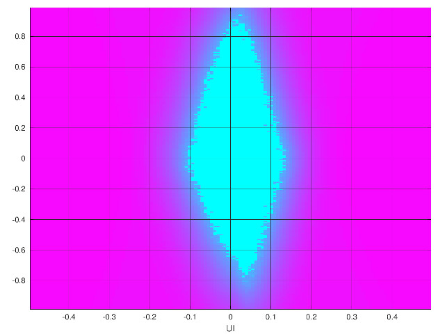
It takes about a minute to obtain an image like this. But it's possible to reach a good assessment of the channel's quality based upon a cruder image that can be obtained in less than a second.
There is usually no need to design anything in order to obtain a statistical eye scan. In particular, this process can be carried out by Vivado with the help of the JTAG connection. Unfortunately, not all MGTs have the capabilities for a statistical eye scan.
This wraps up the fifth page in this series about MGTs. The next page continues discussing the PMA and its capabilities when the regular data stream is turned off.