This page is the forth in a series of pages introducing the Multi-Gigabit Transceiver (MGT). The previous pages discussed the MGT and a few protocols that are used with it, as well as some encoding methods.
Introduction
As already mentioned in the first page of this series, an MGT is just a sophisticated kind of SERDES. Among the reasons for making it sophisticated, there are a few building blocks inside an MGT that helps implementing some specific protocols. This page explains the rationale behind some of these building blocks.
The part in the MGT that contains these units is usually referred to as PCS (Physical Coding Sublayer). This name is misleading, as some of the logic inside the PCS have nothing to do with neither encoding nor decoding.
This is a block diagram of a typical MGT, showing the PCS' position in the larger context.
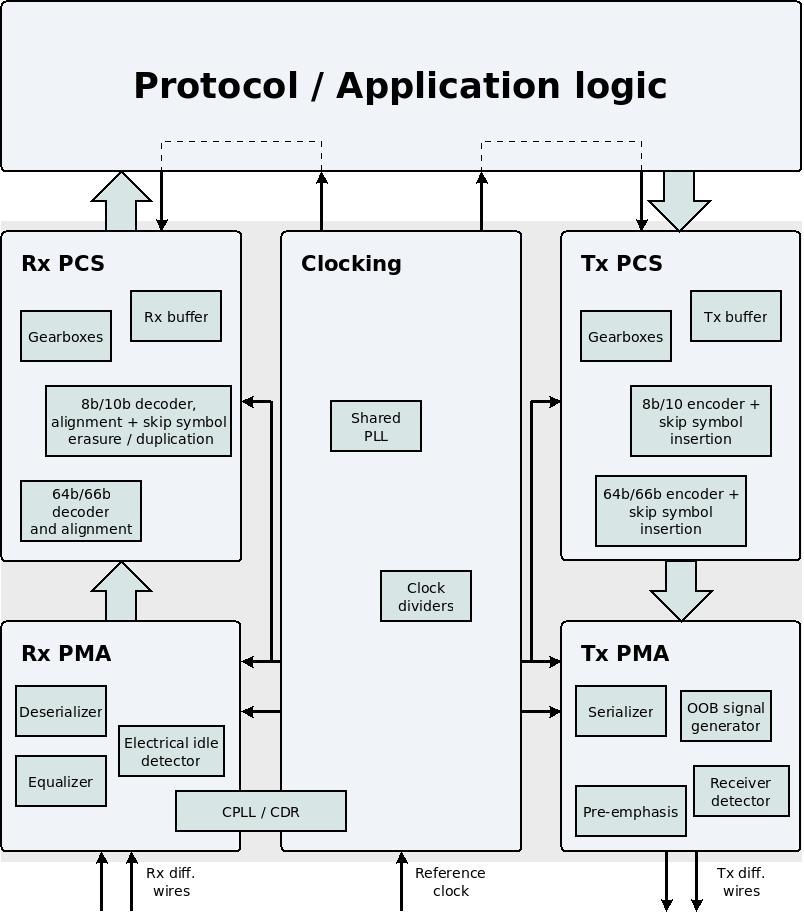
The PCS consists of everything between the PMA and the user application logic. I shall use the expressions Tx PMA and Tx PCS in relation to the parts in the MGT that are used for transmitting data. Likewise, Rx PMA and Rx PCS will be the expressions for the parts used for receiving data.
The Tx PCS begins at the input ports where the application logic hands over the data for transmission to the MGT. The Tx PCS ends its role when there is a parallel word that consists of the bits that are ready for transmission over the physical wires. This parallel word is handed over to the Tx PMA part for the purpose of serializing and conversion to an electrical signal.
Likewise, Rx PCS begins with the parallel word of data that the Rx PMA has received and deserialized, and ends at the output ports where the MGT hands over the data to the application logic.
Since the PCS consists of logic that operates on the parallel word only, it's evident that all of the PCS' functionality can be implemented in the logic fabric. Nevertheless, this logic is implemented inside the MGT for the same reason that many building blocks are implemented in hard IPs. Some protocols take advantage of the PCS' encoding capabilities. Other protocols (e.g. xillyp2p) rely on their own methods for processing the data stream, making the use of the MGT much simpler, as shown in this design example.
As each MGT has a different internal structure, it's impossible to describe the detailed flow of data inside an MGT's PCS in a way that covers all MGTs. The descriptions and explanations below are therefore focused on what the PCS' functional blocks are intended to achieve. The detailed description of a PCS and its building blocks can only be found in the MGT's own documentation. With the explanations below, reading this documentation will hopefully be easier.
Encoding and decoding
Several encoding methods were introduced on the previous page: 8b/10b, 64b/66b, 64b/67b, 128b/130b and 128b/132b.
The implementation of 8b/10b is part of all FPGA MGTs, inside their PCS. The implementation includes the encoding and decoding the 8-bit words into 10-bit words and vice versa, as well as the other features that were mentioned in the previous page: K-symbols, synchronization and alignment in response to a comma symbol (K28.5) and also responding to skip symbols (K28.0).
As for the other encoding methods, each MGT implements a different set of encodings. The MGTs also differ in what features of the encodings are implemented. Sometimes the MGT's PCS implements only the required gearbox, and sometimes the mechanism for automatic synchronization is included as well. There is no standard set of features.
Gearboxes
Throughout the PCS as well as in the interface with the application logic, the data stream on the physical channel is represented with a parallel word. The width of this parallel word may change as the data traverses the different processing steps inside the PCS. For example, when the data passes through an 8b/10b encoder, the word width changes from 8 bits to 10 bits.
However, the interface for transmitting the application data to and from the MGT consists of input ports and output ports having a width that is always a multiple of 8. Typically, this width is one of 16, 32, 40, 64, 80, 128 or 160 bits.
But what happens, for example, if 64b/66b encoding is used? With this encoding, the data stream on the physical channel consists of segments that are 66 bits long each. If this data is presented with a parallel word that is 64 bits wide, the beginning of each segment will appear at a different position in this word every time. Among the allowed widths for the interface with the application logic, none of them avoids this problem.
This is what a gearbox is for. It's a logic module that reorganizes the data that arrives in its input port into a parallel word with a different width.
For example, say that we want to transmit data that has been encoded with an 64b/66b with the help of an MGT, and the encoder is implemented in the application logic. The encoder's output is 66 bits wide, but the MGT's input can be either 64 or 80 bits wide (or other alternatives that are even less relevant). To solve this, we need to implement a gearbox that reorganizes the existing parallel word (66 bits wide) into a word that the MGT can accept (64 bits wide). This is a situation better avoided.
For this reason, MGTs often have one or several gearboxes included in their PCS part. In particular, when the MGT includes a 64b/66b encoder (or similar encoders, such as 128b/130b), there is also a suitable gearbox inside the MGT. This way, the MGT handles all tasks that are necessary for a transmission of encoded data: First, the data is encoded with the MGT's encoder, and then the gearbox changes the parallel word's width so that this word can be handed over to the Tx PMA part for transmission. A similar solution is used for receiving data.
Because the words on each side of the gearbox are different, the number of bits going into the gearbox is different from the number of bits going out of it. If the input's parallel word is wider, the gearbox must occasionally refuse to receive a word in order to compensate for this. Likewise, if the output's parallel word is wider, the gearbox will not always have something valid on its output port. So if the gearbox operates with only one clock, there must also be a flow control signal that compensates for the different amount of bits on each side. In Xilinx / AMD's terminology, this is referred to as a synchronous gearbox.
Alternatively, the gearbox can depend on two clocks. The frequencies of these clocks are chosen to that they compensate for the ratio between the word widths in the gearbox' both sides. The advantage of this method is that the data flow is never stopped on either side of the gearbox. However, a gearbox of this sort requires two clocks and operates in two clock domains. This solution is called an asynchronous gearbox.
Tx buffer (Tx FIFO)
The Tx buffer (often referred to as Tx FIFO) is a small FIFO inside the Tx PCS. This FIFO's depth is usually 16 or 32 data elements, and it is usually half full under normal working conditions. The need for this FIFO is somewhat complicated and is explained below. However, this explanation doesn't answer the only question that is usually relevant when configuring an MGT: Should the Tx buffer be enabled or not?
The answer is that in most cases, the Tx buffer should be enabled. The only reason to avoid using the Tx buffer is if its delay causes a problem: Using a Tx buffer means an unknown delay between the moment a parallel word is handed over to the MGT and the moment this word is transmitted on the physical layer. In most applications, this means an uncertainty of around or less than 0.1μs, so the protocol is indifferent to this delay.
As for why this FIFO is needed, the explanation follows.
There are at least two clock domains inside a Tx PCS: The first clock is used for interfacing with the application logic. The second clock (sometimes called XCLK) is used where the Tx PCS hands over the parallel word for transmission to the Tx PMA.
The subject of clocking inside an MGT is discussed separately on a different page. For now, it's enough to understand why there must be two separate clocks. To explain this, we shall compare the MGT to a regular SERDES.
Say, for example, that we want to transmit data at a rate of 1000 Mbits/s with the help of a regular output pin. Most FPGAs today have a SERDES attached to each output pin for this purpose. For this example, let's assume that the application logic feeds the SERDES with a parallel word that is 8 bits wide. The clock for this parallel word is hence 125 MHz.
Accordingly, the SERDES is fed with two clocks: One 125 MHz clock, and a second clock with a frequency of 500 MHz. The SERDES uses both clock edges of the 500 MHz clock, so the data is transmitted at the desired rate of 1000 MHz.
The two clocks that the SERDES receives must be aligned. For example, the rising edge of the 500 MHz clock must occur at the same time as the rising edge of the 125 MHz clock. This is necessary for the SERDES' proper operation. This alignment is achieved by using one PLL for creating both clocks, and using clock buffers that have the same propagation delay. This is a usual method for ensuring that clocks are aligned: See the explanation about related clocks.
But what if we want to transmit 5000 bits/s? This is too much for a regular output pin, so an MGT is needed. There is a SERDES inside the MGT as well. Let's assume that the parallel word that goes to this SERDES has a width of 32 bits. Accordingly, the clock associated with this word has a frequency of 156.25 MHz. Let's also assume that the interface with the application logic consists of a parallel word that is also 32 bits wide. Hence the clock frequency for this interface is 156.25 MHz as well. But is it the same clock signal?
In order to transmit the parallel word, the MGT's SERDES must be connected to a 2500 MHz clock (a new bit is transmitted on both clock edges). This frequency is too high for the FPGA's general-purpose PLLs. It's also impossible to use the FPGA's clock buffers or other routing resources for this clock. The MGT must therefore has its own PLLs and wires for the purpose of generating the two aligned clocks that the SERDES requires. More details about this in the page about the MGT's clocking.
Now we're in position to understand why there are at least two clock domains inside the Tx PCS. In this example, the Tx PCS feeds the Tx PMA with a parallel word that is 32 bits wide. The clock for this word is 156.25 MHz. This clock is created by the MGT's PLL in order to ensure the alignment with the 2500 MHz clock. The interface between the application logic and the MGT is based upon the exact same clock frequency, but the application logic can't use the same clock signal despite this: The application logic's clock must go through the logic fabric's clock buffer so that this clock reaches all logic elements without any skew. Because of this clock buffer's delay, the application logic's clock is not naturally aligned with the 2500 MHz clock.
The most straightforward way for a clock domain crossing is using a FIFO (as mentioned on a page discussing this topic). The Tx buffer is this FIFO.
MGT's that offer the option to bypass the Tx buffer, also offer other methods to ensure the alignment that is necessary between the clocks inside the Tx PCS. However, these methods are complicated and error-prone.
Rx buffer (Rx FIFO)
The Rx buffer (often referred to as Rx FIFO) is a small FIFO inside the Rx PCS. In principle, this buffer is the same as the Tx buffer, so everything said about the Tx buffer above holds true for the Rx buffer as well. In particular, the answer to whether this buffer should be enabled is the same: The Rx buffer should be enabled in most applications, except for when the delay it causes is unacceptable.
The Rx buffer has an additional purpose, however: It allows the Rx PCS to work with two clocks that have a slight difference between their frequencies. We shall now look at why this difference can occur.
First, let's remind ourselves that this discussion focuses on the part of the MGT that receives a data stream. However, this data stream is generated by another MGT, which relies upon another reference clock (in most scenarios). The MGT that receives the data stream often doesn't have access to the clock used by the transmitter. Instead, the receiver creates a replica of this clock based upon the data stream only (this is called CDR, Clock Data Recovery).
As a result, the Rx PMA works with a clock that adapts itself to the transmitter's data rate. The frequency of this clock is uncertain, within a defined tolerance. The protocol always defines how much the frequency is allowed to diverge from a specified number, but there is always a level of uncertainty.
Hence the interface for handing over parallel words from the Rx PMA to the Rx PCS depends on a clock that adapts itself to the transmitter. The Rx PCS must be synchronous with a foreign clock.
But why is this different from the Tx PCS? Recall from the discussion about the Tx buffer that there are two clock domains inside the part of the Tx PCS. Even though these two clocks aren't the same clock signal, they have exactly the same frequency, because they are based upon the same reference clock.
Likewise, there are two clock domains in the part of the Rx PCS. One of the clocks has an unknown frequency. What about the other clock? The answer is that it depends on the application logic's requirements: In most scenarios, an MGT is used to implement a bidirectional protocol. This protocol involves transmitting data in response to data that is received. It's therefore convenient that all of the application logic is synchronous with one clock. More specifically, the most common solution is that all of the application logic is synchronous with the clock that is used for transmission. This means that the interface between the Rx PCS and the application logic is synchronous with the same clock as for the Tx PCS.
When this approach is taken, the two clocks inside the Rx PCS don't have the same frequency. As a result, the Rx PCS receives data from the Rx PMA at a different rate than it passes this data over to the application logic. The Rx buffer is capable to absorb this difference temporarily: If the application logic fetches data at a slower rate, the Rx buffer will accumulate the surplus. If the application logic fetches data at a faster rate, the Rx buffer is gradually emptied.
This is, of course, a very temporary solution. The Rx buffer will sooner or later overflow or become empty unless something is done to maintain its fill level around half its capacity. There are different mechanisms for this purpose. For example, recall from the previous page that if 8b/10b encoding is used, skip symbols can be inserted in order to compensate for differences between the clock frequencies. The mechanism for taking advantage of skip symbols is implemented inside the Rx PCS: If the Rx buffer is more than half full, the Rx PCS doesn't write skip symbols into the Rx buffer. This reduces the fill level. On the other hand, if the Rx buffer is less than half full, the Rx PCS reads the skip symbols from the Rx buffer repeatedly. As a result, new data fills the buffer at the same time as this buffer isn't drained. Hence the Rx buffer's fill level increases.
The Rx buffer is often called an elastic buffer because of this capability to temporarily absorb differences in its fill level. It's important to note that this capability is not always needed: If the application logic interfaces with the Rx PCS with a clock that has the same frequency as the Rx PMA's clock, the Rx buffer behaves in principle the same as the Tx buffer. When this approach is taken, the application logic is responsible for implementing the clock domain crossing, if such is necessary. This approach also allows to disable the Rx buffer if necessary (in order to avoid the delay in particular). Xillyp2p is an example of application logic that receives the data with the Rx PMA's clock, but allows for using the Rx buffer in order to simplify clocking.
Features related to pseudo-random sequences
A pseudo-random bit sequence (PRBS) is a sequence of bits that appears to be random, however it isn't really random: A PRBS repeats itself periodically. As it's easy to generate a PRBS with very long periods (several millions bits), the statistical properties of a PRBS resemble those of a truly random sequence of bits.
The most commonly way to generate a PRBS is with the help of a Linear-Feedback Shift Register (LFSR). This logic consists of a few flip-flops and XOR gates, so an LFSR doesn't require a lot of resources to implement. An example for a commonly used LFSR can be found in a separate page that discusses a mathematical topic related to LFSRs.
The PCS part in an MGT usually has a few features related to PRBS. In particular, the MGT may have an implementation for a scrambler. When the synchronization of the scrambler is implemented in the Rx PCS, this can save a lot of work.
Another very common use of a PRBS is testing the physical channel for errors. This is a useful method because the receiver can easily generate the correct sequence of bits with the help of an LFSR. Errors in the physical channels are detected by comparing the bit sequence that is generated locally with the arriving data stream. This mechanism is not difficult to implement in the logic fabric, but some MGTs have this capability built-in nevertheless.
Unfortunately, the physical channel can't be used for transmitting data while an error test is performed with the help of PRBS. It is therefore impossible to monitor the channel's quality while it is actually used. Some protocols have mechanisms for reporting errors, but usually an error is reported only if it disrupted transmitted data. One exception is xillyp2p, which also reports errors that occur when the link is idle.
This wraps up the forth page in this series about MGTs. The next page starts discussing the PMA and its abilities to compensate for difficult physical channels, as well as its ability to perform eye scanning.