This page is the first in a series of pages introducing the Multi-Gigabit Transceiver (MGT), and an overview of what's to come in this series.
Introduction
Multi-Gigabit transceivers (MGTs) play an important role in the communication between different parts inside a computer or an electronic system. Several well-known interfaces inside a computer are based upon MGTs, for example PCIe and SATA. Other well-known interfaces are used for communication between a computer and its peripherals, for example Gigabit Ethernet, SuperSpeed USB, Thunderbolt and Displayport.
MGTs are also used to connect between electronic components, for example between two FPGAs. In this case, the communication is often based upon one of the less known protocols, or even a non-standard protocol. But it's also possible to use MGTs for connecting an FPGA with another type of component, or between other components among themselves.
For example, fiber optic transceivers are often standard modules (in particular in SFP+ form factor) that interface directly with MGTs. Some high-speed ADC/DACs also use MGTs in order to transfer the sample data (usually based upon the JESD204 protocol). Some protocols are intended for transferring video data (e.g. some of MIPI's protocols for the physical layer).
Even though MGTs are often used for bidirectional protocols, each MGT consists in fact of two independent parts: A transmitter and a receiver. It is hence possible to use an MGT for a unidirectional transmission by turning off one of the two parts. With most FPGA MGTs, it's also possible to configure the parameters of the transmitter and receiver independently.
In summary, MGTs are used in many applications. Often, the name of the interface doesn't imply that MGTs are used (e.g. Gigabit Ethernet, SATA and DisplayPort), but the physical layer consists of MGTs.
It's worth mentioning that Xilinx (and then AMD) calls their MGTs by different names: RocketIO, GTX, GTH, GTY, GTP, GTM, etc. Each name represents a specific hardware implementation of the transceiver, so this name says something about the data rates and other performance attributes that the transceiver has.
This series of pages explain the basics of MGTs and a few commonly used technical terms in the relation to them. The purpose of this is to make it easier to read the technical documentation, and in particular, to be able to recognize which parameters are relevant to your project, and which are not.
What is an MGT?
It's important to realize that behind all the complicated features, an MGT is just a SERDES: It's an electronic building block that receives and transmits data. The MGT's electrical interface with the physical world consists of two wires that constitute a differential pair. When the voltage on the first wire (the "plus" or "positive" wire) is higher than the voltage on the other wire (the "minus" or "negative" wire), the physical state corresponds to a '1'. Otherwise, it's a '0'. This is the same principle as with differential interfaces, such as LVDS.
Another similarity with a SERDES is that the MGT's interface with the application logic consists of a parallel word: For each cycle of the application logic's clock, a number of bits are transmitted between the application logic and the MGT. This arrangement is necessary as the data rate is much higher than the maximal clock frequency that is possible for an FPGA.
There are, however, a few important differences between a usual SERDES and an MGT. These are a few of them:
- The MGTs are capable of data rates much higher than those of a regular SERDES.
- The receiver of a SERDES needs to be given the transmitter's clock along with the data stream. An MGT receiver, on the other hand, can rely on the data stream's signal alone: The MGT creates a clock that matches the data stream's signal and uses this clock instead. This capability is called clock data recovery, CDR. Even if an MGT receiver has access to the transmitter's clock, it is used only as a reference clock, and not as the data clock itself.
- Bit errors are allowed and normal on a data link that uses an MGT. The BER is usually expected to be below 10-12 or 10-15. If a bit error occurs on a regular SERDES, it's considered a malfunction, but not so with an MGT.
- When an MGT is used, there are restrictions on the content of the data stream that is transmitted on the pair of electrical wires. The data stream is always required to be DC balanced. In other words, the number of '0' and '1' on the data stream must be equal on the average. Also, it is often required that the transmitted bits are statistically independent of each other. More about this below.
- An MGT is capable of producing and detecting out-of-band signals (OOBs). These signals are transmitted when the regular data flow is shut down for saving energy. The purpose of these signals is primarily to wake up the receiver on the other side in order to resume the transmission of data bits.
So why is an MGT so complicated?
Anyone who has attempted to configure an MGT block for an FPGA project knows that there are a lot of parameters and choices. Why does it have to be this way?
There are mainly three reasons for this: First, because the MGT block implements many building blocks that can be implemented in the logic fabric, but are implemented as part of the MGT for efficiency. For example, all MGTs have the capability to encode and decode 8b/10b, even though this task can be performed by the application logic. But since this encoding technique is so commonly used, the MGT has the capability to handle it instead.
The second reason is related to clocking: There are several clocks required for an MGT's proper operation. To make things even more complicated, the requirements on the clock's quality (jitter in particular) are tighter, in comparison with the clocks used for the FPGA's logic fabric. And sometimes SSC (Spread Spectrum Clocking) is also used, which makes things even more complicated.
So getting the clocking done right is sometimes no less difficult than choosing the correct parameters for the MGT in general.
The third reason is that MGTs are designed to support several standard communication protocols. Consequently, the names of features that are needed for a specific protocol are often taken from the protocol's specification. Such jargon means nothing to someone who doesn't know the relevant protocol. This makes it difficult to decide which features to enable when setting up an MGT block for an FPGA.
All of these topics are discussed in more detail in the rest of this series of pages.
Things to be aware of
In most use cases, MGTs are used as the physical layer for another well-established protocol, in particular PCIe. In these situations, the FPGA tools take care of the details, and there's no need to understand much on what happens at the low level.
However, if you intend to connect your application logic directly to an MGT, it's important to be aware of several challenges that this logic will need to tackle. Some of these issues are handled by protocols intended for use between FPGAs.
This is a short list of topics to take into account. Each of these topics are discussed in more detail in the rest of this series of pages.
- Word alignment: Just like with any SERDES, an MGT doesn't have prior knowledge about where a byte or a larger word begins. With a SERDES, this problem is usually solved with trying to move the parallel word by one bit at a time (bit slipping), until the arriving data stream makes sense. Protocols that are based upon MGTs usually rely upon a synchronization word for this purpose.
- The bits on the physical wires must be DC balanced. The easiest solution is to use 8b/10b encoding, but there are other and sometimes more suitable possibilities.
- Scrambling: It's almost always a good idea use an equalizer on the receiving MGT. The equalizer compensates for the physical media's imperfections, and by doing so it reduces the BER. This is true in particular when the data rate is high, when low-cost cabling is used or when the physical distance is long. However, some types of equalizers require that the transmitted data is statistically random: No correlation between one bit to another is allowed in the transmitted data stream. The common solution is to use a scrambler, which performs a XOR between the payload data and a pseudo-random sequence of bits. The receiver performs XOR with the same pseudo-random sequence and obtains the original data stream this way.
- Bit errors: The data may arrive with errors to the receiving MGT. The logic that consumes this data must be designed to cope with such errors. In some applications, the errors are deemed rare enough to be ignored (for example when transmitting raw video data and the BER is below 10-15). In other applications, an error detection and/or retransmission mechanism is required to ensure that the data link is reliable.
- Differences between clock frequencies: When an MGT receives a data stream, this signal is based upon the other side's clock (i.e. the transmitter's clock). This clock may have a slightly different frequency compared with the clock available on the receiver's side. However, the interface between the MGT and the application logic is often based upon the local clock. Hence if the transmitter's clock is faster than the receiver's clock, this means that the MGT receives data faster than it is able to deliver this data to the application logic. As a result, this excessive data accumulates inside the MGT block and eventually some kind of overflow occurs. Conversely, if the arriving data rate is lower than the local clock, the MGT can't deliver data on each clock cycle. These problems occur even if the reference clock is passed from the transmitter to the receiver along with the data stream: Slight fluctuations in the clock's frequency are enough to cause problems of this sort. The protocol usually solves this problem with the help of idle words.
- Energy consumption: MGTs tend to consume a lot of power. This is partly because of the high data rate, and often the high-quality PLLs turn out to waste a lot of energy. Therefore, it is often desirable to shut down an MGT when it's not used, even for very short periods. For example, a SuperSpeed USB link often turns off its data stream if no data has been transmitted for a time period as short as 50μs. An OOB handshake is then used to resume operation when needed.
PMA, PCS and clocking
This block diagram shows the parts of an MGT as well as its interaction with the application logic:
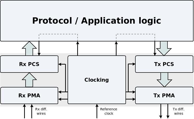
The functionality of an MGT is usually divided into three parts:
- Clocking: As mentioned above, an MGT's operation requires several clocks. Even though the FPGA tools configure these clocks' parameters automatically, it's nevertheless necessary to be aware of how these clocks are generated.
- PMA (Physical Medium Attachment): This part contains the MGT's SERDES as well as the analog-signal subsystems (OOB signals, receiver detection, equalizer, pre-emphasis etc.). This part also implements the CDR.
- PCS (Physical Coding Sublayer): This part contains logic that can be helpful for implementing the communication protocol: Encoders and decoders, word alignment, gearboxes, FIFOs, etc. Most of the functionality in the PCS can be implemented in the logic fabric instead, but is implemented inside the MGT for simplicity and efficiency.
These topics are discussed further in this series of pages.
The PIPE interface
The PIPE standard is worth mentioning: This standard defines the connections between an MGT and the logic that implements PCIe, SuperSpeed USB or SATA. This includes the ports that are used for communicating the data, control signals and status signals.
In this standard, the MGT is referred to as the PHY layer, and the protocol is called the MAC layer. This terminology is also used by standards that define Ethernet, USB 1.x and USB 2.0. These standards are usually implemented by two separate chips. For example, in order to implement Ethernet on a processor chip, the MAC layer is implemented in this chip, and the PHY layer is implemented in a separate chip. The PIPE standard is written in the same spirit, even though PCIe, SuperSpeed USB or SATA are practically always fully implemented on the same chip. The connections between the MAC layer and the PHY layer that are defined by the PIPE standard take place inside the chip, and are rarely visible to the outside world.
An important impact of the PIPE standard is that a decent FPGA MGT always implements the PIPE interface as required for PCIe. The PIPE interface for SATA is also often supported. This is obviously useful when implementing these two protocols, however there is another important benefit: Different FPGAs have a similar interface with the MGT. In particular, there are some functional elements that can be found in practically all MGTs.
Conclusion
An overview of the MGT and its complexity was presented on this page. In the rest of this series of pages, many of the concepts mentioned above are explained. But before that, we shall start with a short outline of protocols that are often used when connecting two FPGA MGTs.