This page is the seventh in a series of pages introducing the Multi-Gigabit Transceiver (MGT).
Introduction
It's natural to expect that most of the work with configuring an FPGA's MGT would relate to the processing of the data and choosing the correct protocol. It may therefore come as a surprise how much time and effort is required to get the clocking right. Most of this effort is usually spent on sorting out the different options that the MGT offers in relation to its clock resources as well as the restrictions that they impose.
As design rules in relation to the MGT's clocks are different on each FPGA, the only reliable source for accurate and comprehensive information on this topic is the MGT's own documentation. Such documentation usually focuses on the mechanisms and their details, and may not explain why these mechanisms are necessary. This page attempts to fill in this gap by discussing the concepts and challenges related to the clocks used by an MGT.
PLLs and VCOs
Generally speaking, PLLs multiply the frequency of a reference clock with a constant. This constant is sometimes an integer, but it can also be a fractional number, and it can also be smaller than 1. In other words, the frequency at a PLL's output can be lower than the reference clock's frequency. This is rarely the situation with PLLs that are used with MGTs, but this can be useful with PLLs for the logic fabric.
In an FPGA, there are separate PLLs for the purpose of generating the clocks required for the MGTs. The PLLs and other clock resources that belong to the logic fabric aren't capable of supporting the frequencies required for an MGT. In particular, the MGT requires a clock whose frequency is at least half the data rate. For low data rates, the required frequency may be higher.
For example, if the data rate is 5 Gb/s, the bit clock will usually run at 2.5 GHz. This is because the MGT's SERDES is activated by both clock edges (DDR). However, if the data rate is relatively low, the output of the MGT's PLL may be divided into a lower frequency.
Almost all PLLs work according to the same principle: The central part is a VCO (Voltage Controlled Oscillator) that can generate a clock having a range of frequencies. The VCO's output is inserted into a clock divider which divides the frequency by a constant number. The output of the clock divider is compared with the PLL's reference clock. A control mechanism adjusts the VCO's frequency so that the reference clock and the clock divider's output are aligned. In other words, these two signals have the same frequency and the same phase.
Going back to the example with 5 Gb/s, let's assume that the reference clock's frequency is 125 MHz. A possible implementation for a PLL is that the VCO's output is divided by 20. The divided signal is compared and aligned with the reference clock. Hence the VCO's frequency must be 2500 MHz, because 2500 MHz / 20 = 125 MHz.
This method for creating a clock is suitable for transmitting bits: The transmitting MGT decides alone where each bit's time period begins and ends. However, when the MGT receives bits, the other side dictates each bit's timing. Hence, the receiver needs to adapt to the arriving data stream. As mentioned in one of the previous pages, this adaption mechanism is called Clock Data Recovery (CDR). The implementation of CDR consists of a control loop which adjusts the VCO's frequency for the purpose of synchronizing the receiver's clock to the arriving data stream. The reference clock is used occasionally in order to put the VCO at an initial frequency that is close enough to the expected frequency. The reference clock is ignored after a synchronization has been achieved.
Utilization of PLLs
The PLLs for MGTs inside an FPGA is a complicated topic. Each MGT can receive its clock from more than one PLL. If there is only one application that uses MGTs in the FPGA project, the tools usually choose the most suitable PLL automatically. However, if the MGTs are used for different purposes in a project, it's important to ensure that each MGT is connected to the PLL that is most suitable.
In an FPGA, there are usually PLLs that are shared between a number of MGTs. AMD (Xilinx) calls these QPLL, and Altera has fPLL and ATX PLL. On the other hand, there are PLLs that are local to a specific MGT. These are called CPLL (AMD / Xilinx) or CMU PLL (Altera). The local PLLs usually have a lower quality and less capabilities, compared with the shared PLLs. The differences can be the range of frequencies, jitter, and which multiplication ratios can be chosen in relation to the reference clock.
Each FPGA has a set of complicated rules that define how the PLLs and the MGTs can be interconnected. These rules also define the possibilities to connect the PLLs to the FPGA's reference clock inputs. It's therefore not possible to take for granted that all MGTs can be connected to the clocks that they need. This is very different from the logic fabric's clocks, for which there is there are almost no restrictions.
It's hence recommended to read through the datasheet carefully before making decisions on which PLL to choose for each MGT. In particular, it's important to verify that it's possible to provide all MGTs with their clocks when designing a PCB. This can be done by creating an FPGA project that includes all required MGTs, and ensure that this project's implementation is successful and that all pins are placed in the correct positions.
Reference clock
The FPGA has separate pins for the reference clocks that are intended for the MGTs' PLLs. In a PCB design, it's important to verify that a reference clock input can be used with the MGTs for which the clock is intended. The interconnect between reference clock inputs, PLLs and MGTs doesn't allow all possible combinations. The allowed combinations are described in the FPGA's documentation, but it can be difficult to reach a definitive conclusion, as the rules can be complicated. It's often better to ensure that the needs are covered with the help of FPGA projects.
The clocks used for this purpose must have a high quality in terms of accuracy and low jitter. It's a common mistake to connect a clock that is generated by a general-purpose clock chip. Doing so will probably degrade the MGT's performance, and create faults that look like signal integrity problems or added noise on the data wires.
If the MGT is intended for a specific protocol (e.g. PCIe, SuperSpeed USB or SATA), it's recommended to read the FPGA manufacturer's documentation about the reference clock's requirements. Several electronic components that are labeled as a "low-jitter clock source" may not be good enough.
Jitter is a random process. The jitter's magnitude is an important parameter, but not always a sufficient one. The randomness of the clock's jitter can cause fast changes in the clock cycle, and these changes can also be slow. How the jitter behaves in this regard can be deduced from the jitter's noise spectrum.
The datasheet of the component that creates the clock sometimes only gives a number for the magnitude of the jitter (usually measured in picoseconds). Information about the jitter's noise spectrum is often unavailable. It's possible that such a component is adequate despite this absence of information, in particular if the jitter's magnitude is extremely low anyhow. There is often no simple answer to this question.
The reference clock's quality is nevertheless important for any use of the MGT. The well-known protocols' requirements are a good reference that can be used in any project. It's also useful to compare with components that are used as reference clocks on development boards.
Clocks for the logic fabric
The clock that is used for the interface between the MGT and the logic fabric originates in the MGT's own PLL. This is necessary, because inside the PMA the SERDES relies on two clocks: The clock corresponding to bits on the physical channel, and the clock that is used along with parallel words. For the SERDES to work properly, these two clocks must be aligned inside the PMA.
On the other hand, any clock that is used by the logic fabric must be distributed in a way that ensures a low clock skew. A global clock buffer is often chosen by the tools for this purpose. The propagation delay from the clock buffer to all logic elements is almost equal, so the clock's edges arrive simultaneously to all destinations. This is a necessary condition for allowing the tools to perform proper timing calculations with regards to the logic fabric.
Even though this propagation delay is uniform across all wires, it's not necessarily small. On the contrary, the wires inside the FPGA that connect the clock buffer to its destinations add a considerable delay. This doesn't usually matter, because the differences between all these connections are small.
But this delay makes the two clocks that are used by the PMA unaligned with the logic fabric's clock. It's impossible to align these three clocks with the help of the logic fabric's resources, because one of these clocks has a frequency that is too high. And yet, the MGT and the logic fabric must have a clock that both sides are synchronous with. The only solution is to add another clock signal.
This boils down to that there must be at least three clock signals involved for each direction:
- The clock that is synchronous with the bits on the physical channel. This clock's frequency is often half the data rate (2.5 GHz in the example from above).
- The clock that is synchronous with the parallel word inside the PMA. This clock is sometimes referred to as XCLK. For example, if the PMA interfaces with the PCS with a parallel word that is 32 bits wide, this clock is 156.25 MHz (because 5000 / 32 = 156.25).
- The logic fabric's clock: This is the clock used along with the interface between the MGT and the logic fabric. This clock usually has names like TXUSRCLK2, RXUSRCLK2, tx_coreclkin, rx_coreclkin and other similar names ("Tx user clock" and "Rx user clock" in the diagram below). This clock's frequency depends on the width of the parallel word used to interface with the logic fabric.
Note that there are separate clocks for transmission and reception in general. This block diagram shows the typical distribution of clocks inside an MGT:
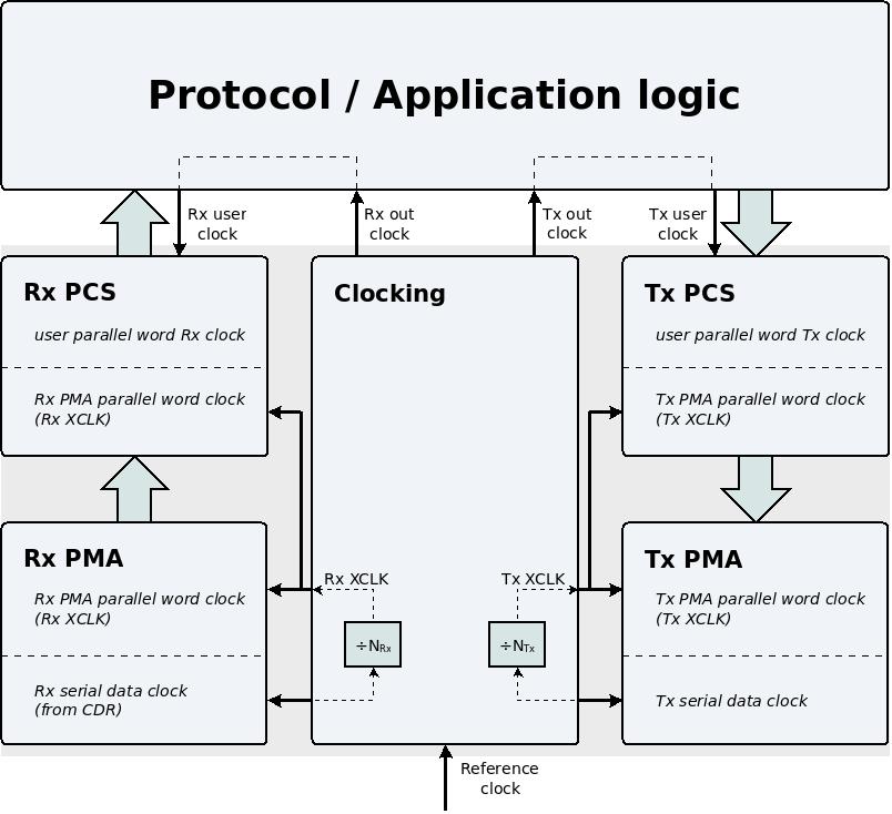
In this block diagram, there are four clocks for each direction, not three as mentioned above. This is explained next.
Generating the logic fabric's clock
As explained above, the clock that is common to the logic fabric and the MGT must be distributed with the logic fabric's clock buffer. On the other hand, this clock must originate from inside the MGT.
We shall start with the simplest possible solution to these two conflicting requirements: The MGT indeed generates a clock and makes it available at an output port. This output port is usually called TXOUTCLK, RXOUTCLK, tx_clkout, rx_clkout etc. (this is the forth clock, named "Tx out clock" and "Rx out clock" in the diagram above). This signal goes into the input of a logic fabric clock buffer. The output of this clock buffer is the clock signal used for interfacing between the MGT and the logic fabric.
As a result of this arrangement, the only difference between the logic fabric's clock and the clock generated by the MGT is the propagation delay of the clock buffer. In other words, the MGT has full control over the logic fabric's clock, except for its phase. This is important in particular for receiving data, if the CDR's clock is used as a basis for the interface with the logic fabric (this option is discussed below). This is because the CDR continuously adjusts this clock's frequency in order to remain synchronized with the arriving data stream.
As discussed in a previous page, the PCS offers mechanisms for overcoming the difference between the phases of the logic fabric's clock and the PMA's clock. The Tx buffer or Rx buffer are the easiest choices, but the PCS may also have the capability to adjust this difference directly.
But which clock is exposed on the MGT's clock output port? The natural answer is XCLK, because this clock is the closest candidate to the requirement on the logic fabric's clock. There are however several other possibilities for generating the logic fabric's clock. For example, the MGT's clock output can be fed into a regular logic fabric PLL in order to generate a clock that has a different frequency. This PLL is used together with a clock buffer, so the clock signal is adequate for its purpose. Using a PLL this way opens new possibilities, for example that the MGT passes through its own reference clock at its clock output port. The frequency of this clock may not be correct for using the clock for the interface with the MGT, but the PLL can multiply this clock by the necessary ratio.
Also note that the frequency of the logic fabric's clock can be different from XCLK's frequency. This can be required when an asynchronous gearbox is activated inside the PCS. In this scenario, the frequency difference is required to compensate for the different widths of the parallel word in the PMA and in the interface with the logic fabric.
The rules related to this topic are complicated and different from one FPGA to another. A large part of an MGT's documentation is often dedicated to detailing the different possibilities. Unfortunately, making the correct decisions on clocking requires spending time on learning the rules that apply to the specific FPGA.
Choice of logic fabric clock for receiving data
When choosing how to generate the logic fabric's clock intended for the reception of data, a fundamental decision is required: Whether this clock is derived from the CDR's clock or from a fixed reference clock. In other words, if the logic fabric's clock is adapted to the exact data rate of the arriving data stream or not.
In most applications, the MGT is used for communication of data in both directions. There is often a close relationship between the arriving data and the data transmitted. For example, the transmitted data stream may include acknowledgements and requests for retransmission that are sent in response to the arriving data stream. In applications of this sort, it is convenient that all logic is synchronous with the same clock (i.e. all logic is in the same clock domain). In particular, The PIPE interface requires that all interfaces with the MGT are synchronous with a single clock (named PCLK in the standard document). Recall from earlier that PIPE is the standard interface between MGTs and several protocols: PCIe, SuperSpeed USB and SATA.
This convenience comes with a price, however: The frequency of the logic fabric's clock is potentially slightly different from the frequency used with the PMA's parallel word (i.e. XCLK's frequency). This difference causes a surplus or a shortage of data inside the PCS, because the logic fabric receives the parallel words slower or faster than these words arrive to the PMA. The solution to this is often to use the Rx buffer and skip symbols, as discussed on the page about PCS.
Alternatively, the logic fabric's clock can be derived from the PMA's clock. With this method, the logic fabric consumes the data at the same rate as it arrives. This is the natural solution when the MGT is used only to receive data. It is also a possible choice for a bidirectional link when the application logic takes care of the clock domain crossing. Xillyp2p is an example of a protocol that has taken this approach, as shown in its complete design example.
AMD FPGA: Two clocks from the logic fabric
MGTs on AMD FPGAs (formerly Xilinx) have two clock input ports from the logic fabric, i.e. two ports for each direction: TXUSRCLK and TXUSRCLK2 for transmission, and RXUSRCLK and RXUSRCLK2 for reception. An example of an instantiation of the MGT is presented in this design example.
Almost all interface with the logic fabric is synchronous with TXUSRCLK2 or RXUSRCLK2 (depending on the direction). The other two inputs, TXUSRCLK and RXUSRCLK are used only internally in some parts of the PCS.
TXUSRCLK is often the same clock signal as TXUSRCLK2. However, the MGTs in AMD's FPGAs have a feature that allows the parallel word used in the interface with the logic fabric to be double as wide as inside the PCS. When this feature is used, TXUSRCLK's frequency is double the frequency of TXUSRCLK2. This is yet another reason for using a logic fabric PLL.
The same principle applies to RXUSRCLK and RXUSRCLK2.
Summary
This page has briefly highlighted a few topics related to an MGT's clocks. It is nevertheless necessary to learn about the MGT's specific features and limitations in order to make wise decisions about the utilization of the MGT's clocking resources. Hopefully, the explanations in this page help with understanding how an MGT's clocks are supposed to work and interact with each other.
This wraps up the seventh page in this series about MGTs. The next page finishes this series with a discussion about flow control.